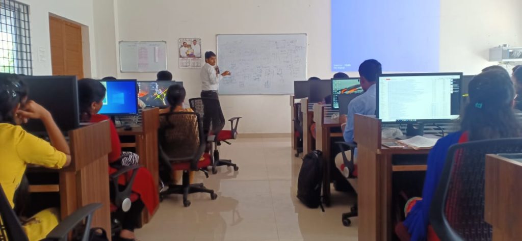
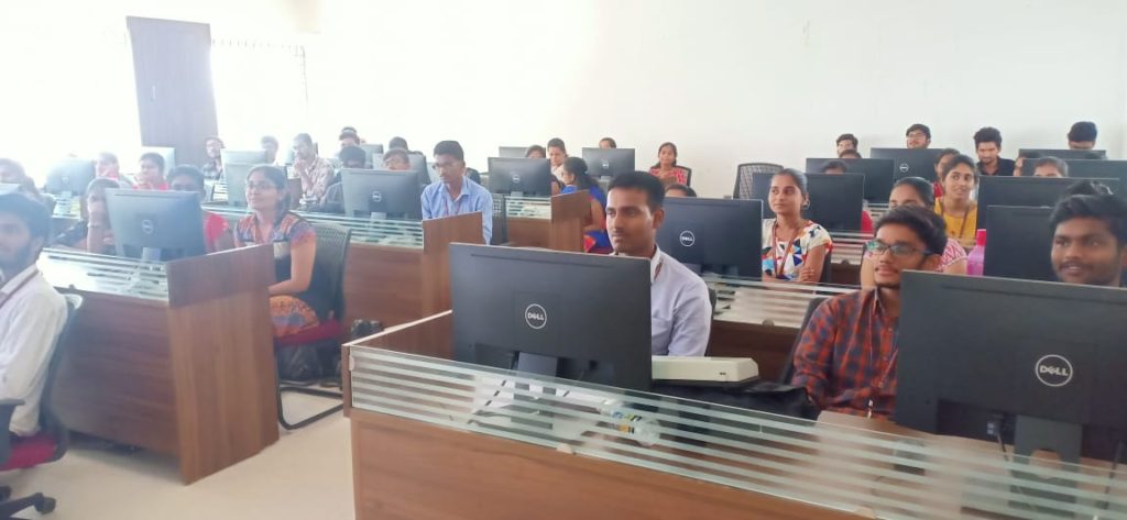
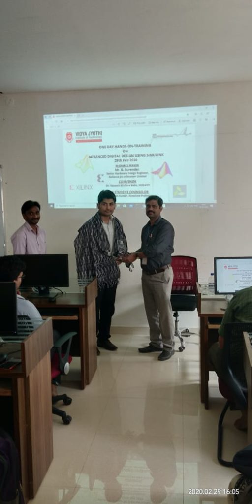
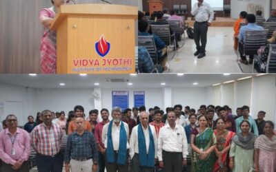
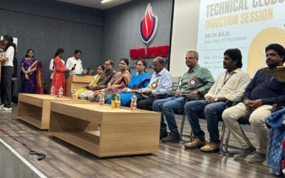
The hands on training on Advanced Digital System Design Using Simulink was organized by IEEE Student Branch, VJIT, Hyderabad held at the ECE Department on 29th February 2020. A total of 48 participants have participated in this training. The participants were from the field of Electronics and Communication Engineering.
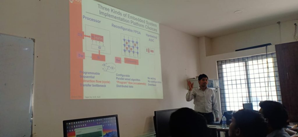
The session started with a lecture on use of FPGA boards in various fields by Mr. G. Surender, Senior Hardware Engineer, JIO Mumbai. The session provided the insights of FPGA architecture and design etc. He also guided us to understanding the different FPGA families and their advantage depends upon application to application. In addition, he also discussed FPGA memory elements. The session I concluded with the internal structure of BRAM design and he also shared his experience in the industry.
The second session started with a lab experiment. The concepts which were discussed in session I were implemented in the lab session. The students designed BRAM in a Vivado system generator. The students learned the importance of the IP integrator and how it can be used at a system level. The students understood the flow chart of Digital System Design. Finally, the students created their own IP block in Vivado to implement their design. At the valedictory ceremony, the participants were awarded the certificates.



0 Comments